Introduction
Generative AI (GenAI) is transforming industries, necessitating the development of specialized hardware to manage its computational demands. AI accelerators or AI chips crafted specifically for AI tasks are critical in this advancement, but designing effective AI chips presents significant challenges.
Certain applications hinge on the absolute criticality of every millisecond—these are known as latency-critical scenarios. For example, latency is crucial in high-frequency trading environments, where algorithms execute transactions in microseconds to leverage fleeting market opportunities. Similarly, cloud services are committed to maintaining 99-percentile latency guarantees to ensure stable and predictable performance, even during peak loads.
Another critical measure is the throughput, which is directly related to the performance of the AI application. One traditional method to manage high computational throughput is batching, where large amounts of tasks are grouped and executed consecutively. However, this technique typically sacrifices latency for throughput, which is a critical trade-off.
Equally critical, yet often overlooked, is flexibility: the balance between memory and compute operations at the system level. Text-based Large Language Model (LLM) operations are memory-intensive, relying heavily on frequent RAM access to manage the vast array of parameters that underpin their linguistic functions. In contrast, Text-to-Video applications demand robust compute capabilities to manage intensive graphical processing and real-time data handling effectively. To support such a diverse array of applications, an AI chip must adeptly navigate the demands of both memory and computational intensity without compromise.
In sum, an effective AI chip must find the sweet spot between latency, throughput and flexibility.
Flexibility and High Utilization
In designing our chip, we prioritized flexibility and high compute utilization to address these key challenges. By adopting a CGRA (Coarse-Grained Reconfigurable Array) architecture, the processing element tiles can be programmed and reprogrammed to carry out a variety of functions, maximizing its flexibility. We also kept the utilization rate high, so that tasks are processed continuously with minimal idle resources, directly enhancing efficiency and reducing latency.
Built on a flexible architecture, ATOM™ leverages synchronization mechanisms to activate resources precisely when needed, to support its powerful parallelism. The time and effort to reach operational readiness is minimized, leading to reduced latency. Moreover, its robust multi-layered memory hierarchy provides significant bandwidth, reducing data dependency, while the sophisticated synchronization lessens control dependency. These features together optimize resource utilization, significantly boosting overall performance and efficiency in a seamless integration.
ATOM™: System-on-Chip for AI Inference
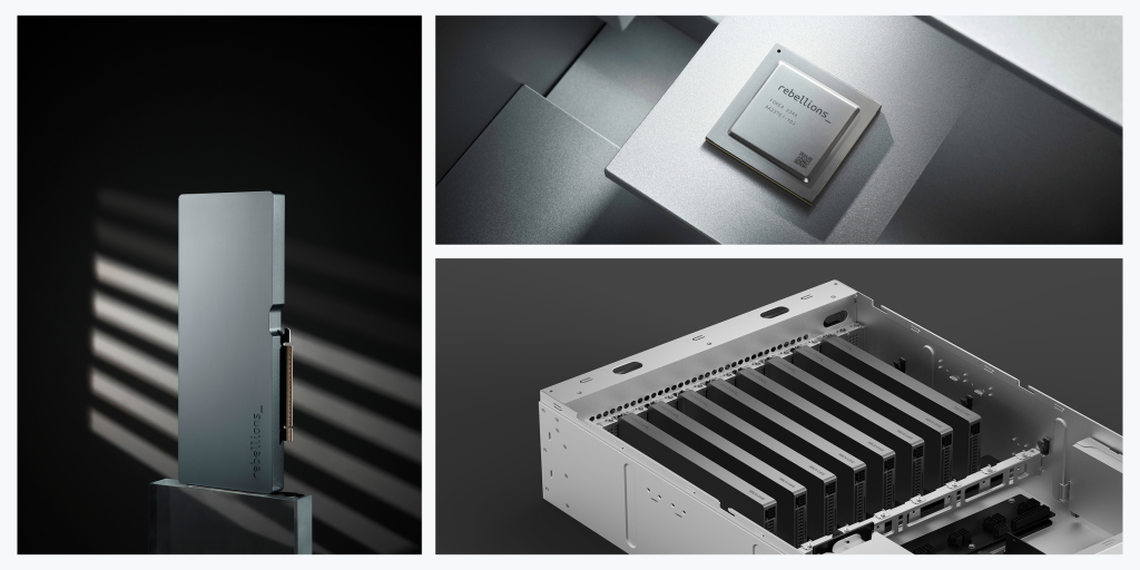
Rebellions’ ATOM™ is an AI accelerator engineered specifically for AI inference tasks with formidable capacity, manufactured on Samsung’s advanced 5nm process. It delivers 32 Tera Floating Point Operations per Second (TFLOPS) for FP16 and 128 Trillion Operations Per Second (TOPS) for INT8, enhanced by eight Neural Engines and 64 MB of on-chip SRAM. With an intricate memory architecture engineered with unparalleled technical mastery, ATOM™ is designed for high performance and peak efficiency.
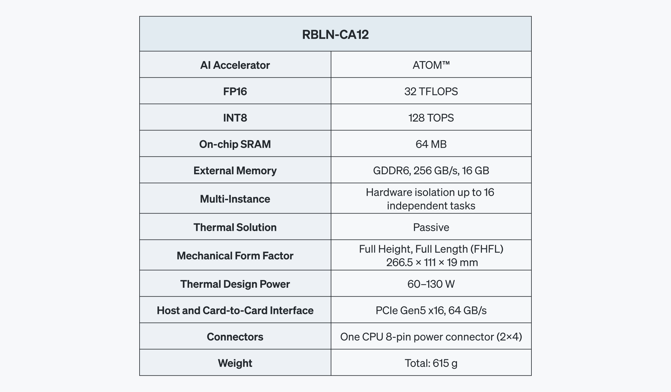
RBLN-CA12
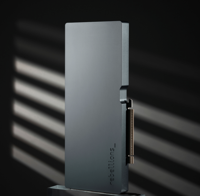
ATOM™ comes in RBLN-CA12, a single slot, FHFL (Full Height, Full Length) PCIe Gen5 card with a TDP (Thermal Design Power) of 60-130 W. RBLN-CA12 features 16 GB of GDDR6 memory with a bandwidth of 256 GB/s and host and card-to-card interfaces via PCIe Gen5 x16. It also has the Multi-Instance capability, partitioning ATOM™ into 16 independent hardware-isolated instances, allowing a dynamic allocation of resources and powerful multitasking.
ATOM™ SoC
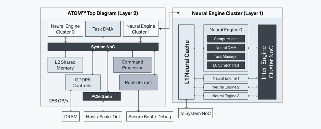
ATOM™ is a multi-core System-on-Chip, consolidating all essential components onto a unified substrate. As shown in Figure 1, this architecture integrates Neural Engines, the Command Processor, shared on-chip memory (SRAM), and GDDR6 memory within one compact surface. The high degree of integration not only diminishes physical footprint but also optimizes power efficiency.
While this configuration in itself ensures streamlined inter-component communication and significantly reduced latency, it is further supported by a sophisticated Network-on-Chip (NoC) that provides high bandwidth. The architecture is also designed to support synchronizations between multiple layers.
Neural Engine
ATOM™’s Neural Engine is where the actual computations take place. The compute units within the Neural Engines incorporate a blend of heterogeneous Single Instruction, Multiple Data (SIMD) and Multiple Instruction, Multiple Data (MIMD) compute elements, harnessing their respective capabilities for parallel performance and dependency control across diverse computational scenarios at the instruction levels.
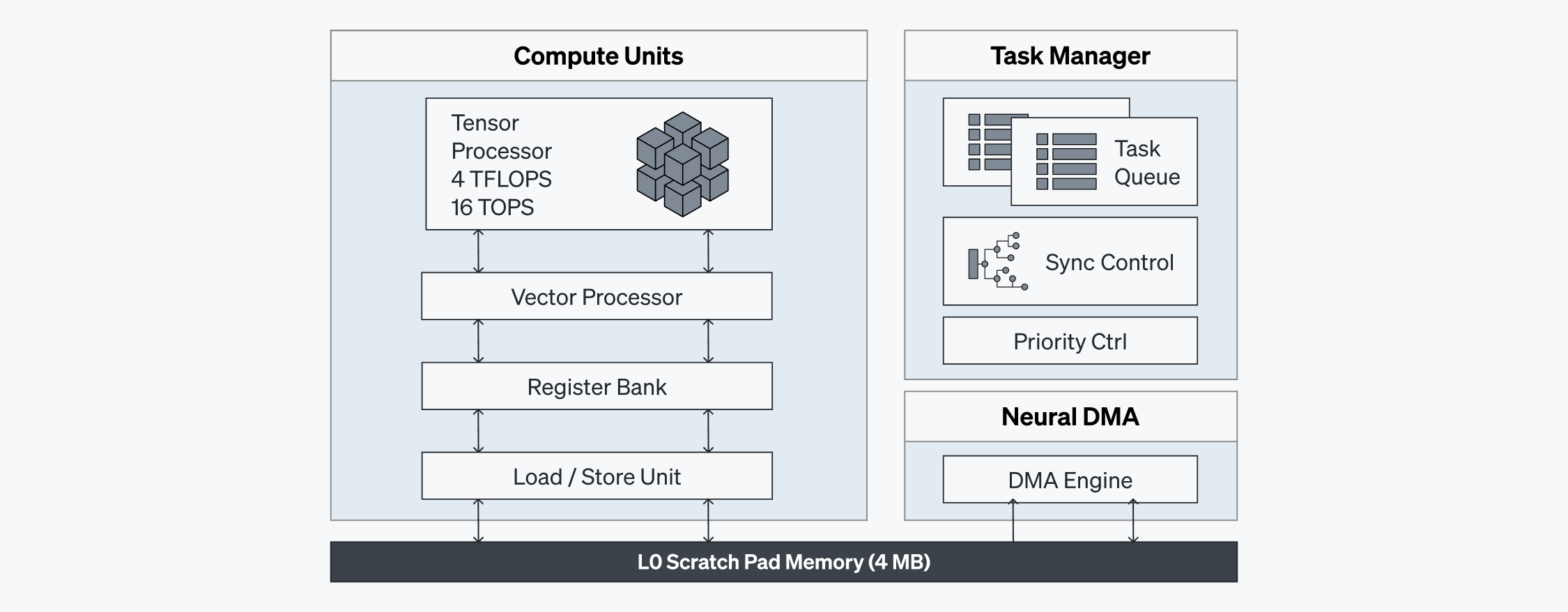
The compute units are fortified with a 4 MB Scratch Pad memory, facilitating access to interim data in the SRAM at a speed up to 8 TB/s. This design mitigates bandwidth limitations and reduces latency by minimizing reliance on off-chip memory sources, thereby optimizing performance and energy efficiency.
Task Managers reside in each Neural Engine to accelerate synchronization on the local hardware level, effectively working alongside the Command Processor in bringing about maximum compute utilization.
The compute units, Scratch Pad memory, and Task Managers within the Neural Engines collectively contribute to ATOM™’s high utilization and low latency performance.
Hierarchical Memory Subsystem
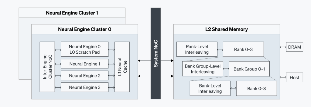
ATOM™’s multi-layered memory architecture is designed to ensure peak performance efficiency, delivering ample bandwidth for the Neural Engines while preserving minimal latency.
At the foundation, a dedicated 4 MB Scratch Pad (L0) within each Neural Engine facilitates immediate local data access. The L1 Neural Cache, located close to the Engines, provides faster access to data. The L2 Shared Memory, a 32 MB SRAM, employs multiple levels of interleaving to support parallelism, optimize bandwidth, and minimize latency. Finally, ATOM™ integrates 16 GB of GDDR6, ensuring high throughput with lower power consumption.
Multi-level Synchronization and Parallelism
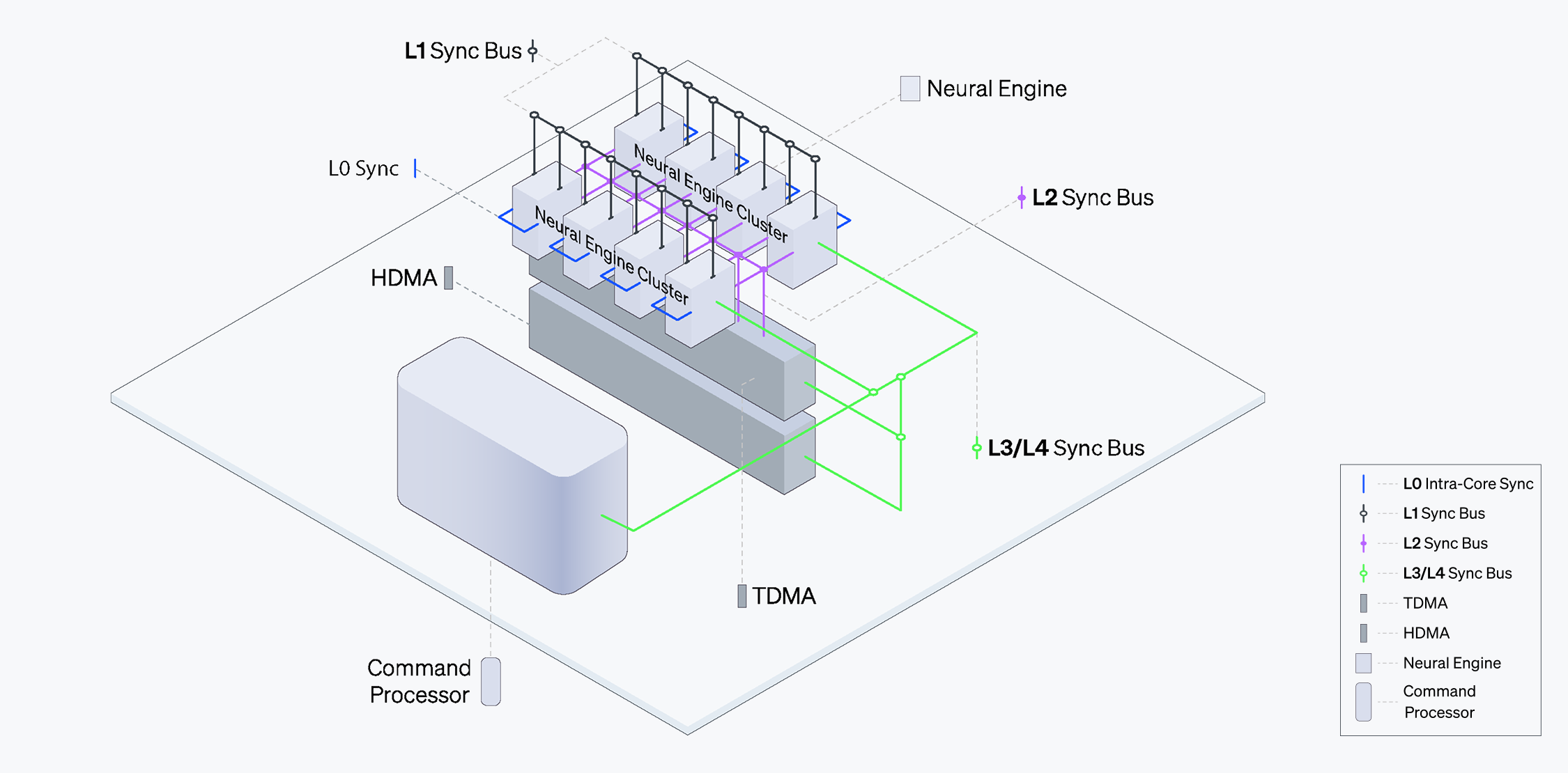
ATOM™’s advanced synchronization mechanisms effectively support parallelism, allowing the chip to scale its performance. Synchronization takes place both at the instruction and task levels, enabled by Command Processors and Task Managers and dedicated local buses that ensure smooth flow through reliable bandwidth.
Neural Engines communicate through Task Managers across the L1 Sync Bus for instruction-level inter Engine communication. Neural Engines Clusters, which consist of four Neural Engines, are connected to the Task Direct Memory Access (TDMA) through the L 2 Sync Bus. TDMA and the Host Direct Memory Access (HDMA) are linked to the Command Processor via L3 and L4 Sync Bus, respectively. This arrangement allows the system to globally check for dependencies, synchronizing different Engines and thereby allowing for the dense compute operations.
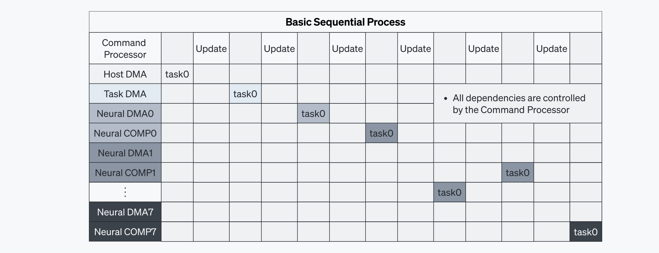
In a basic configuration where the Command Processor solely governs command execution, tasks are processed sequentially, leading to high latency. In Figure 5-1, each task can only be executed once its dependency is resolved by the Command Processor, resulting in a slow and inefficient process. There is communication overhead, critically impacting latency and necessitating further optimization.
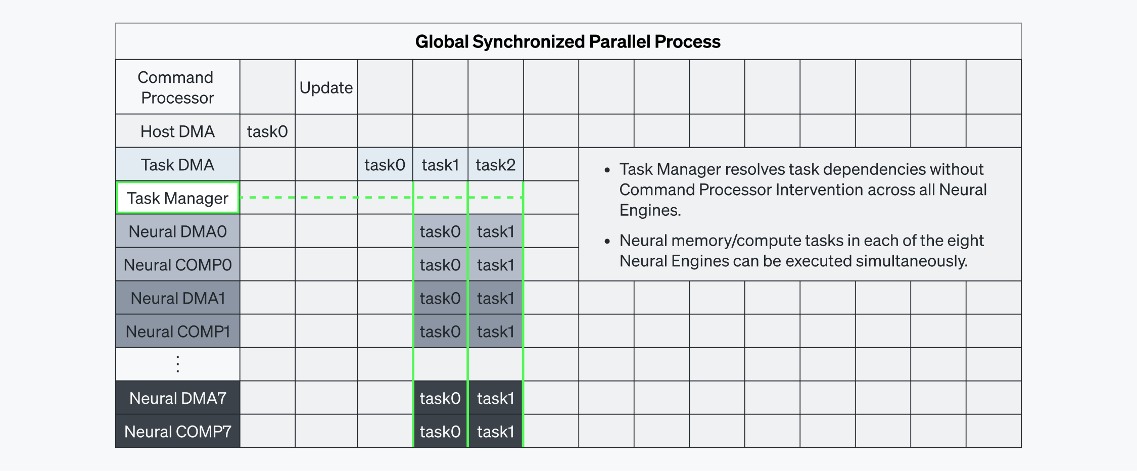
To address this, we introduced Task Managers that autonomously resolve local dependencies directly at the hardware level. In Figure 5-2, the DMA/COMP tasks, each belonging to a Neural Engine, can be executed at the same time, in parallel, without having to wait for the Command Processor to resolve their dependencies. The Task Manager resolves dependencies across all Neural Engines, allowing the tasks to be executed simultaneously. This process is made possible by the dedicated L1/L2 data paths designed explicitly for this purpose, as shown in Figure 4. Consequently, tasks across all Neural Engines are coordinated efficiently, enabling smooth parallel execution and achieving minimal latency.
Benchmark Results
To demonstrate ATOM™’s inference performance for GenAI use cases, we conducted performance measurements on the T5-3B and SDXL-Turbo models, which are renowned for their applications in Natural Language Processing and Text-to-Image Generation, respectively.
These tests were carried out against NVIDIA’s A100, which serves as an appropriate competitor for evaluating ATOM™’s capabilities in the market. By focusing on prominent GenAI use cases, we provide a clear and direct comparison of how ATOM™ stands against existing solutions in handling cutting-edge AI tasks.
Language Model Benchmark: T5-3B
Introduced by Google, the T5, or Text-to-Text Transfer Transformer, is a groundbreaking Large Language Model that leverages the architecture of the widely-utilized Transformer. T5 models are offered in configurations ranging from 60 million to 11 billion parameters.
For our demonstration, we deployed the 3 billion parameter model, which is versatile enough for tasks such as language translation, text summarization, answering questions, and text generation. The test was conducted on batch size 1.
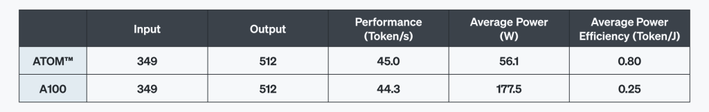
The resulting metrics—performance, quantified by tokens generated per second; power consumption, measured in watts; and power efficiency, calculated as performance per watt—reveal that ATOM™ achieves up to 44% greater power efficiency compared to the A100. This not only underscores ATOM™’s robust capabilities but also its superior efficiency in harnessing computational power for complex language processing tasks.
Text-to-Image Model Benchmark: SDXL-Turbo
SDXL-Turbo, a Text-to-Image model developed by Stability AI, excels in generating high-resolution images and offers significantly faster inference speeds compared to standard stable diffusion models. This advancement has catalyzed the adoption of diffusion-based image generation for practical
applications.
Testing results indicate that ATOM™ consumes considerably less power than the A100 while still delivering high-quality outputs. This efficiency demonstrates ATOM™’s capability to achieve superior results with fewer resources, markedly reducing operational costs and enhancing sustainability in service deployments, as energy consumption is a critical factor that directly influences the Total Cost
of Ownership (TCO) for service providers.

ATOM™’s result is based on projected data. A100’s result is based on the Hugging Face diffusers library.
Conclusion
As businesses are increasingly dependent on AI services, finding the right AI chip that can scale sustainably presents a formidable challenge. The ideal AI chip must strike a precise balance between flexibility, power efficiency, and high performance, without sacrificing latency. ATOM™ has been designed from the ground up to meet these demands, utilizing a CGRA architecture to ensure adaptability and high compute utilization. Its innovative Neural Engines, advanced multi-layered memory architecture, and robust synchronization capabilities optimize both latency and power efficiency. Furthermore, benchmark tests with T5-3B and SDXL-Turbo models demonstrate that ATOM™ delivers up to 44% greater power efficiency than NVIDIA’s A100. These results highlight ATOM™’s capacity to drastically reduce Total Cost of Ownership (TCO) and enhance profitability for AI services, establishing it as the optimal AI chip for a sustainable AI service.


Share This: