

By Rebellions
We have learned a lot from the first real decade of trying to co-design AI hardware to work well with fast-changing AI models. Many different architectures have been advanced to support early machine learning, current GenAI chatbots, and evolving agentic AI workloads, which are all different but which are also similar in that they are highly synchronous across compute engines and their memories. Moreso than even traditional HPC simulation and modeling applications, which laid much of the foundation for artificial intelligence to advance.
AI workloads are sensitive to latency and memory bandwidth, and are at different stages of training and inference, are sensitive to memory capacity, too. The advent of HBM stacked memory has solved the bandwidth problem to a certain extent, but capacity is still an issue. In many cases, the raw flops in a GPU from Nvidia or AMD has too little HBM memory capacity to keep it fed locally on the GPU package, which is why KV caches are being offloaded to a new Tier 1.5 storage that is based on DPUs with locally attached flash.
AI training is largely a solved problem, with Nvidia and AMD providing systems based on GPUs and a mix of scale up networks inside the rack, providing memory coherence across the AI accelerators, and scale out networks to expand the capacity of the machine. But inference is still a wide open opportunity, and the second generation of AI hardware startups are all trying to reposition themselves to chase inference and have all but given up on trying to take on Nvidia or AMD for AI training. The inference market is much more sensitive to both the latency to generate tokens for GenAI chat and agentic workloads, and they are very sensitive to the cost of generating tokens. Rebellions have taken a clean slate approach to create a hierarchy of on die, in package, and rackscale interconnects that can drive up the utilization of the neural processing units in our Rebel chips while also allowing flexible topologies and scale out capabilities to meet a wide variety of inference approaches in the market.
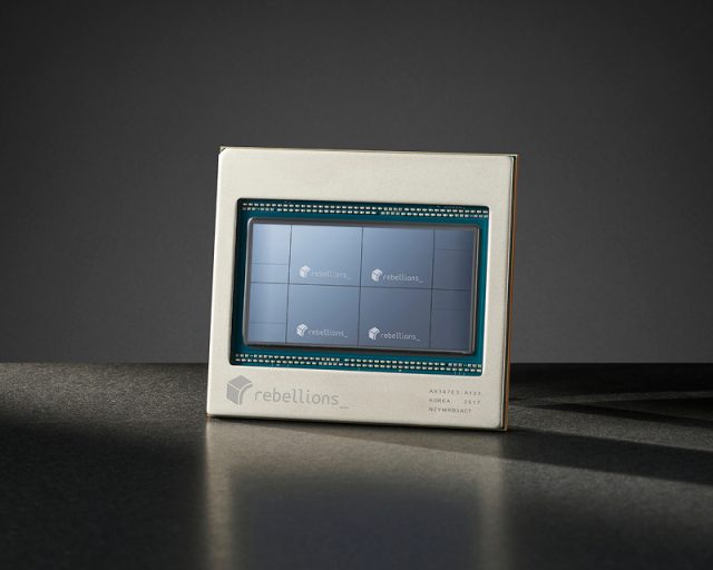
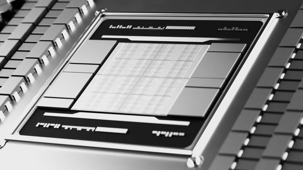
The initial Rebel100™ accelerator, first revealed a year ago at Hot Chips 2025 and also known previously as the Rebel Quad, is a four chiplet complex of neural processing units that uses UCIe-Advanced interconnects to link the four NPUs in the package together.
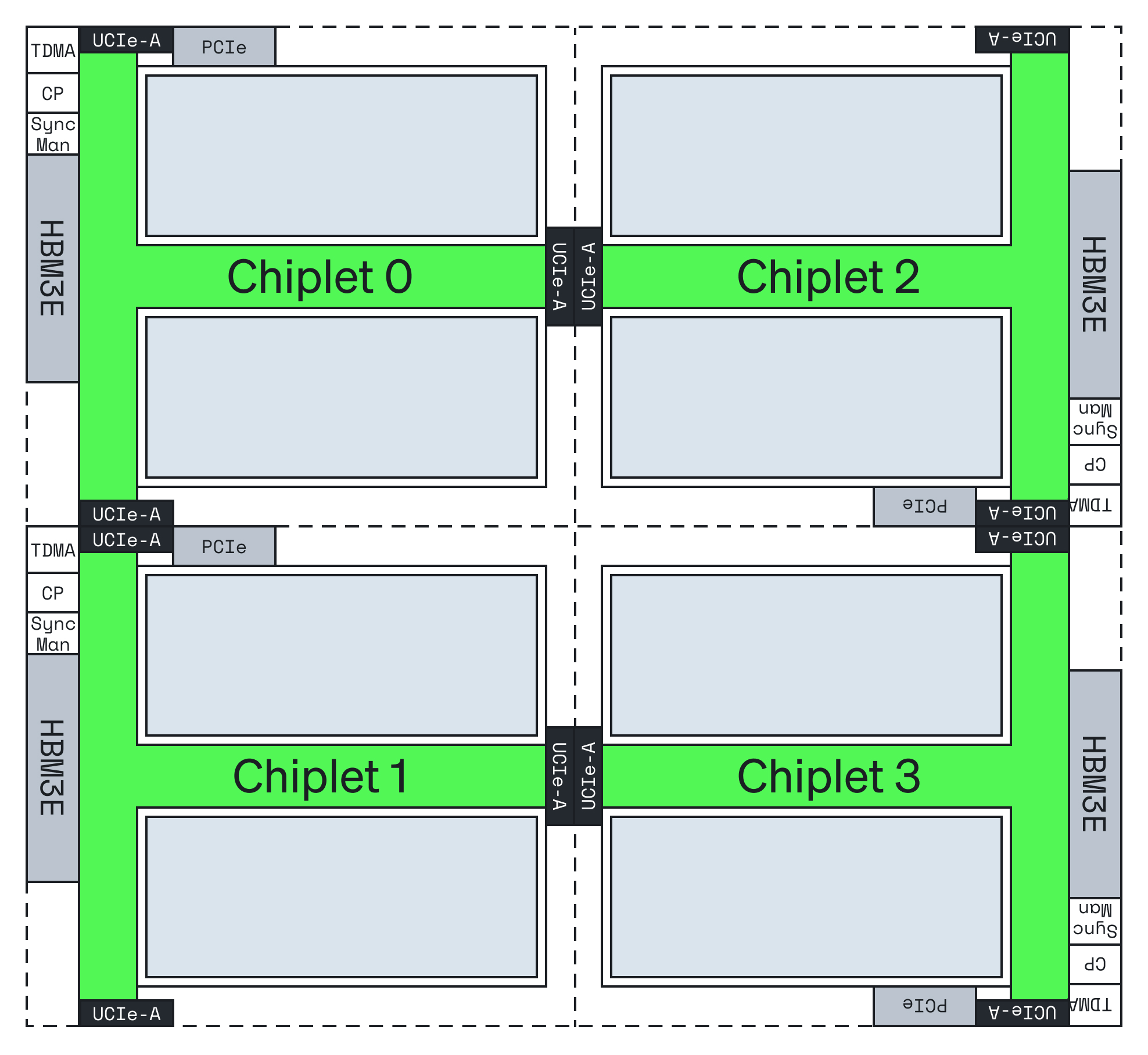
The NPU chiplets are etched using Samsung’s SF4X process, which has 4 nanometer geometries for the FinFET transistors and which is a mature process at this point.
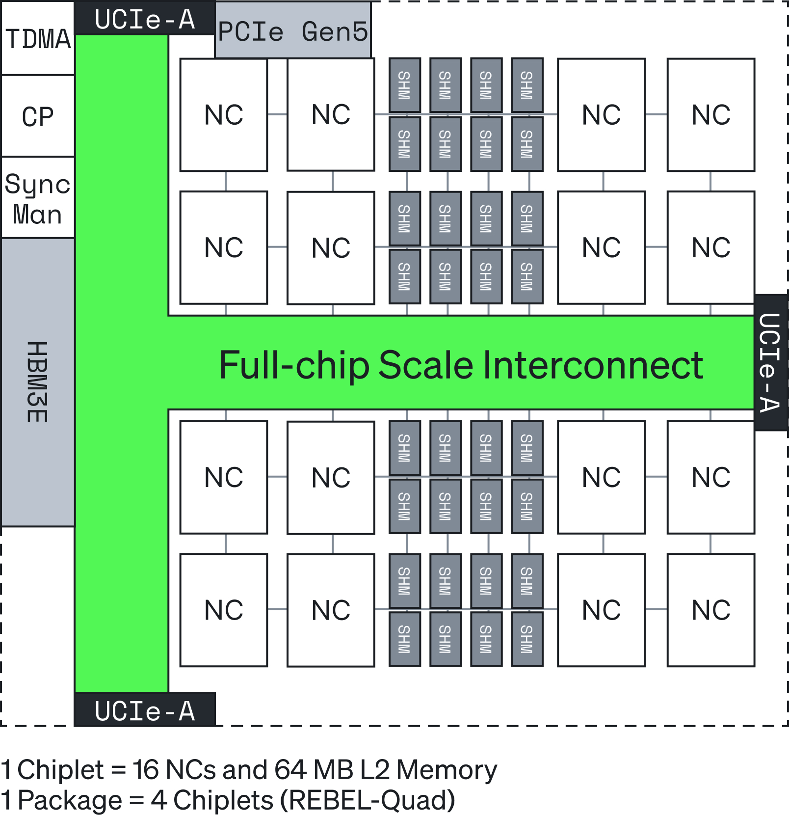
On the Rebel100 chiplet, which is also known as the Rebel-Single, there are 32 L2 memory slices that are interlinked by a shared memory interconnect that is a mesh network on chip that has 16 TB/sec of bandwidth to the L2 slices, which are chopped up into 32 segments for a total of 64 MB per slice. There are 16 neural cores on each Rebel-Single chiplet, each of which has a tensor and vector math unit as well as 4 MB of L1 SRAM.
The Rebel100 package also includes one integrated silicon capacitor (ISC) and one twelve-high stack of HBM3E memory per NPU chiplet. The HBM stacks and ISCs chiplets packaged up using Samsung’s I-CubeS silicon interposer. The HBM3E memory on the Rebel100 has an aggregate capacity of 144 GB and delivers 4.8 TB/sec of aggregate Here is the floor plan of the Rebel IO chiplet:bandwidth, and the UCIe-Advanced die-to-die links provide a virtual monolithic memory space across the four HBM stacks on the Rebel100.
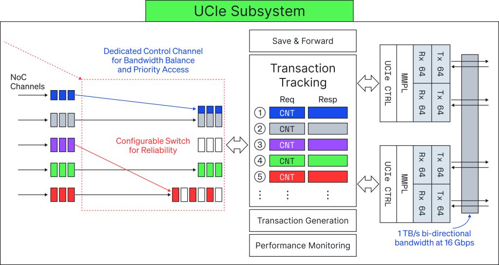
Importantly, the UCIe-Advanced interconnect has a custom implementation of the UCIe protocol, and specifically that UCIe stack has a custom streaming protocol layer and a protocol diagnostics manager that Rebellions created to overcome the limited interoperability and debuggability of standard UCIe. The UCIe customization done by Rebellions also includes multipathing to compensate for UCIe PHY failures. Each chiplet in the Rebel100 has three 1 TB/sec UCIe-Advanced ports – North, South, and East – which link the four chiplets into that virtual monolithic die. The UCIe IPs are licensed from the AlphaWave Semi division of Qualcomm.
The Rebel100 also has two PCIe 5.0 x16 ports, providing host connectivity and peer-to-peer links between multiple Rebel100 devices within a single system.
In terms of performance, the Rebel100 with its quad of chiplets delivers 1 petaflops at FP16 precision and 2 petaflops at FP8 precision.
With the Rebel100s™ follow-on product, we are adding a pair of I/O dies to the complex that provide interconnects to scale up Rebel compute complexes reducing the need for switches – and are doing so with a wide variety of topologies that can match different AI inference engines.
The Rebel100s has four NPU chiplets just like the Rebel100, but now two of the unused UCIe-Advanced ports on the Rebel Single chiplets are used to attach a pair of Rebel IO chiplets, which bring native Ethernet routing and encapsulation of AXI memory protocols using that Ethernet as a transport to tightly cluster compute engines to each other in as many as 256 sockets in the first generation of this integrated interconnect.
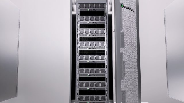
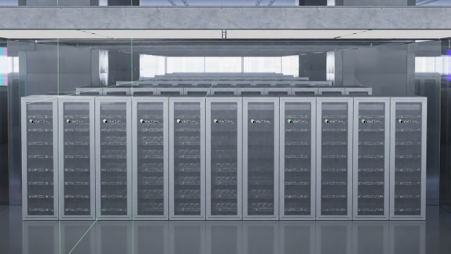
The Rebel IO chiplet has two 16x PCIe 6.0/CXL 3.0 controllers, providing 128 GB/sec of bandwidth, and four Ethernet controllers connected to four Ethernet ports, supporting both scale-up and scale-out networking across up to 256 Rebel100 sockets in a fully configured system. For now, Rebellions is supporting a single rack system with 64 Rebel100s sockets because that is the practical limit with copper-based Ethernet cables. To expand beyond that will require optical cables for some of the links across four racks of machinery.
The routing bus inside the Rebel IO chiplet provides 256 GB/sec of aggregate bandwidth and natively supports 800 Gb/sec scale-up connectivity. For scale-out networking, two 400 Gb/sec RDMA interfaces are grouped to deliver a virtual 800 Gb/sec Ethernet port. Each physical Ethernet port uses eight 112 Gb/sec SerDes lanes. What matters in many cases is that the pair of Rebel IO chiplets can deliver an aggregate scale up bandwidth of 1,600 GB/sec, which is close to the 1,800 GB/sec that Nvidia is offering with the current “Blackwell” B200 and B300 GPU accelerators.
Across the two Rebel IO chiplets, all eight ports can be used to connect up to 64 sockets together without requiring an external switch. For larger configurations, one of the Ethernet ports is used to scale out and the remaining four to seven ports can be configured to create memory server nodes with various topologies. (We will cover the topology options and other features of the new I/O chiplet in a separate blog.) This router is why we do not need switches to make rackscale or even rowscale machines. Normally traffic terminates at the destination port; here, an arriving packet can be relayed – routed back out another port to the next device. Which means that switch functionality is absorbed into the scale-up IO chiplet.
The I/O chiplet has a custom DMA engine that delivers 1 Tb/sec of bandwidth per channel across four channels, and also includes a control processor, a video codec (useful for surveillance applications), and 8 MB of memory for these two units.
The AXI memory protocol to do loads and stores is a homegrown memory semantics protocol that Rebellions developed itself. NPU-generated AXI transactions – meaning loads and stores – go directly onto the Ethernet link. Memory semantics survive across the scale-up boundary; a data master reads or writes a remote device’s address space as a transaction, not a message. An NPU-to-NPU hop across distinct sockets takes about 1 microsecond, and we are working on reducing that to 500 nanoseconds.
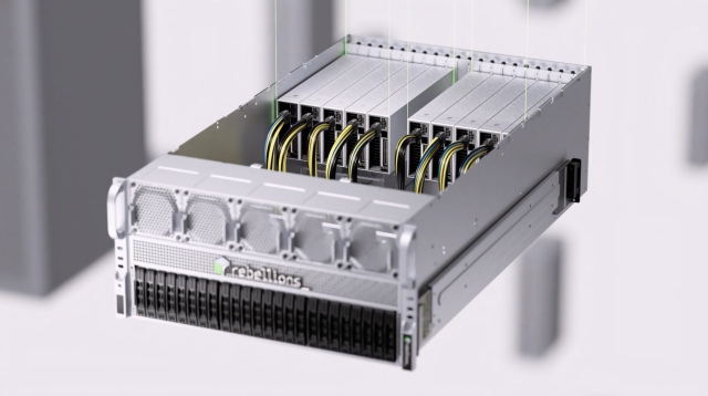
The important thing is this: With rackscale systems based on either Nvidia or AMD GPUs, you have to buy external switches to build a scale up memory domain for the accelerators to share data and work. We have built a distributed switching and routing architecture directly into the Rebel100s socket. This will provide better performance, lower latency, and lower cost than using external switches to make the scale up interconnect. And scale out ports are available to expand beyond a four rack system, which will of course require an Ethernet switch.
Another custom design we are adding with the Rebel100s accelerator is the scale up hardware synchronizer. Without the hardware synchronizer, every time you send data from one Rebel accelerator to another one, there will be some sync point. If there is no sync mechanism, then the destination has to notify the sending NPU that the data has arrived. Then the destination will send another notification to the sender again. That kind of handshake mechanism takes a very long time. So we have implemented our own sync mechanism. So when we send the data, at the end of the data as a post envelope, the sync mechanism will be sent as a serial way, and then once the data is arrived at the destination, the sync also indicates the dependent target to the MPU or some other targets to destination. There is no required handshake between the sender and receiver. This hardware synchronizer is going to provide very high performance for actual inference applications.
In a later blog, we will talk about the various topologies that are possible with the Rebel100s with its integrated I/O chiplets, and what affect this has on inference performance.





Share This: